
We are the present moment, we are love.
-- by Weijun Zhang, July 2001  NEW BOOKS, See the new books on: FPGA, Digital Design: Online Interactive zyBook, HDL, VHDL, Verilog, System-Virlog
Table of Contents
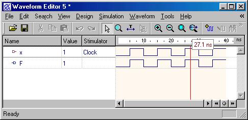
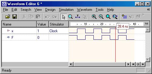
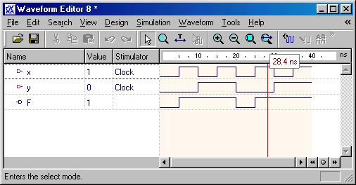
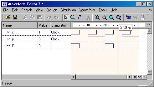
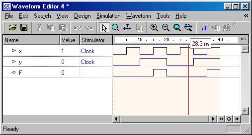
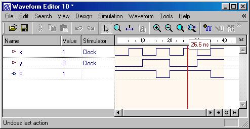
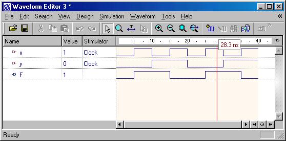
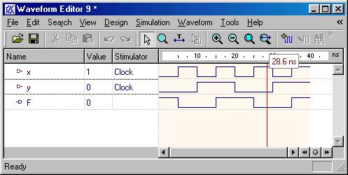
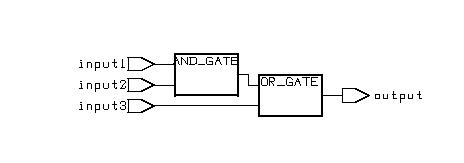
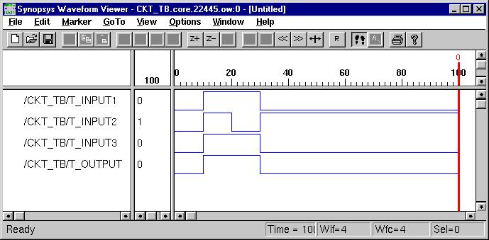
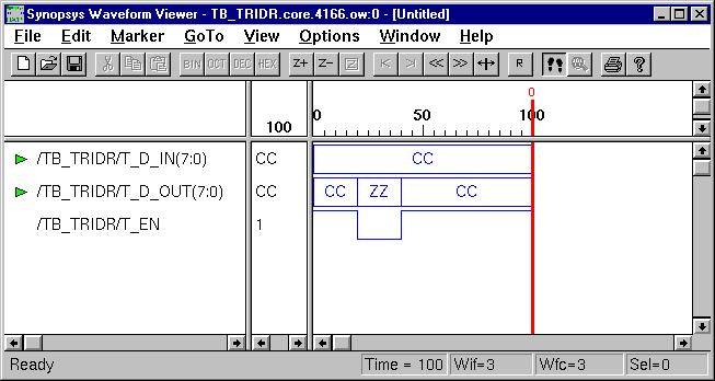
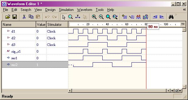
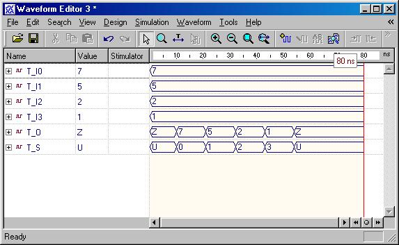
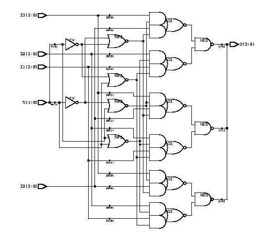
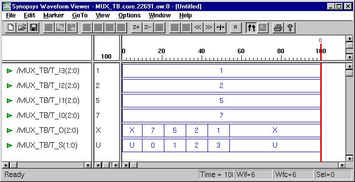
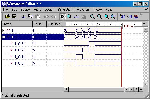
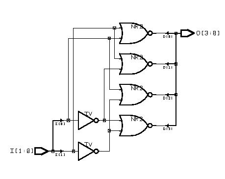
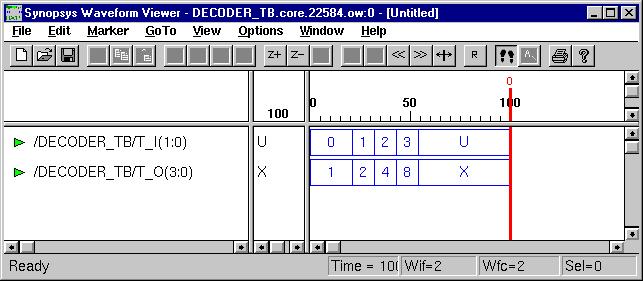
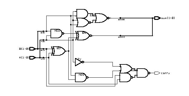
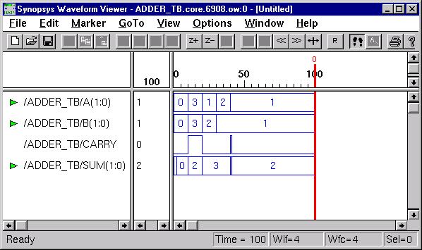
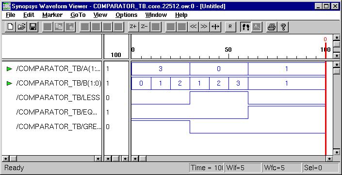
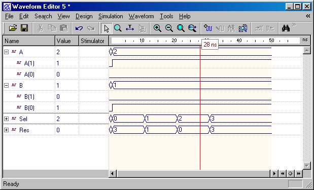
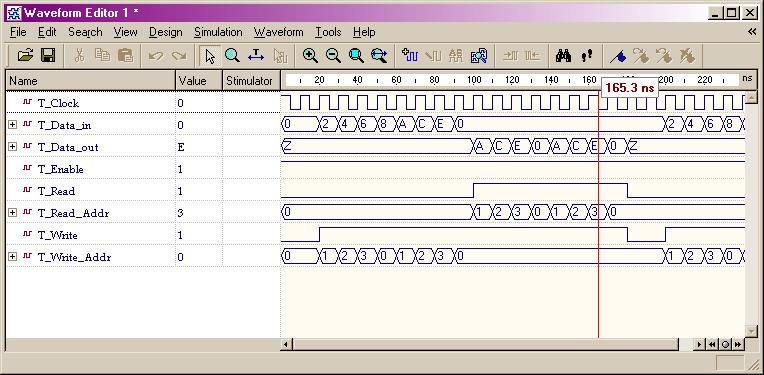
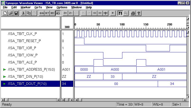
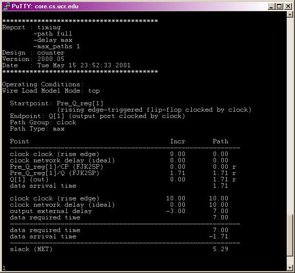
Basic Logic Gates (ESD Chapter 2: Figure 2.3) Every VHDL design description consists of at least one entity / architecture pair, or one entity with multiple architectures. The entity section of the HDL design is used to declare the I/O ports of the circuit, while the description code resides within architecture portion. Standardized design libraries are typically used and are included prior to the entity declaration. This is accomplished by including the code "library ieee;" and "use ieee.std_logic_1164.all;". Combinational Logic Design (ESD Chapter 2: Figure 2.4) We use port map statement to achieve the structural model (components instantiations). The following example shows how to write the program to incorporate multiple components in the design of a more complex circuit. In order to simulate the design, a simple test bench code must be written to apply a sequence of inputs (Stimulators) to the circuit being tested (UUT). The output of the test bench and UUT interaction can be observed in the simulation waveform window.
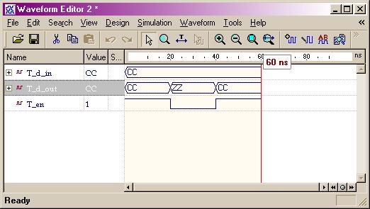
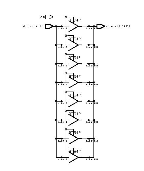
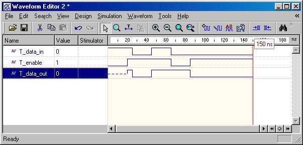
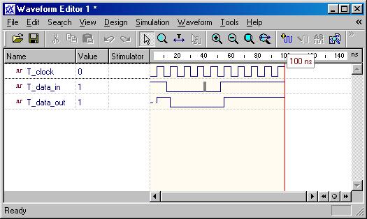
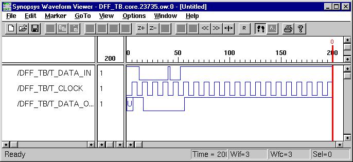
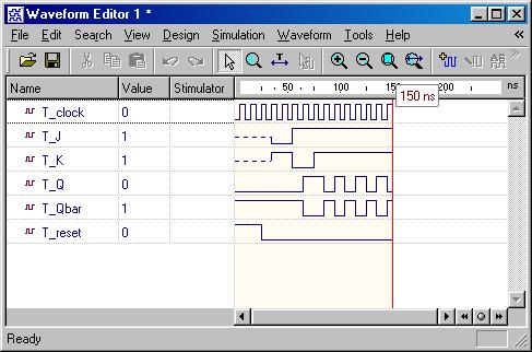
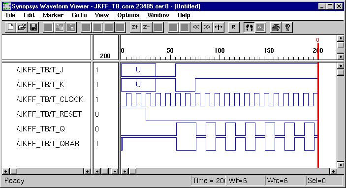
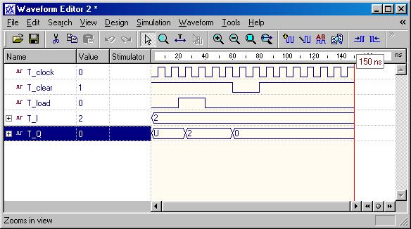
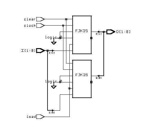
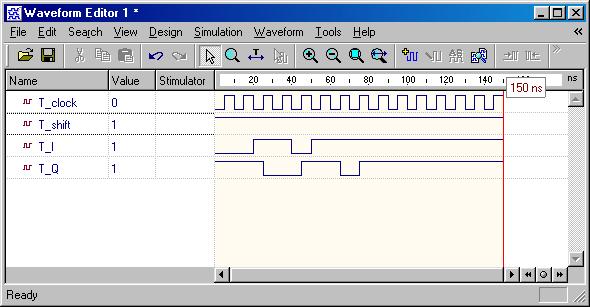
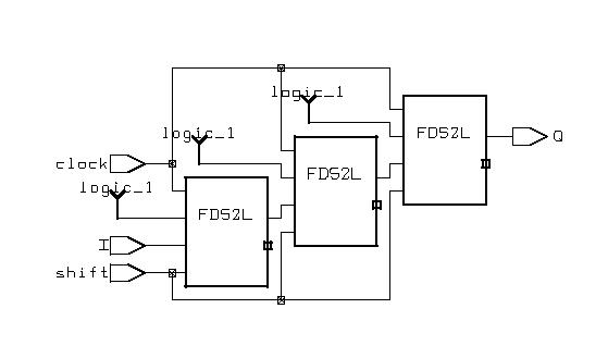
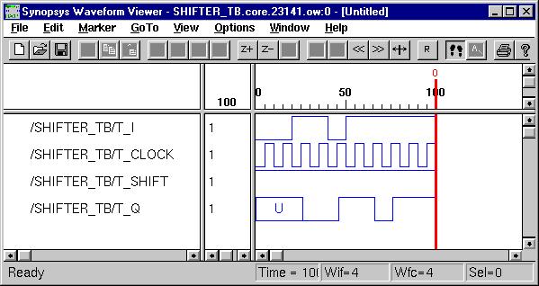
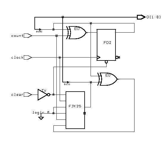
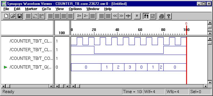
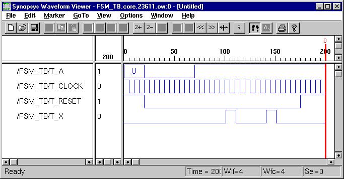
Typical Combinational Components (ESD Chapter 2: Figure 2.5) The following behavior style codes demonstrate the concurrent and sequential capabilities of VHDL. The concurrent statements are written within the body of an architecture. They include concurrent signal assignment, concurrent process and component instantiations (port map statement). Sequential statements are written within a process statement, function or procedure. Sequential statement include case statement, if-then-else statement and loop statement. Latch & Flip-Flops (ESD Chapter 2.3) Besides from the circuit input and output signals, there are normally two other important signals, reset and clock, in the sequential circuit. The reset signal is either active-high or active-low status and the circuit status transition can occur at either clock rising-edge or falling-edge. Flip-Flop is a basic component of the sequential circuits. Typical Sequential Components (ESD Chapter 2: Figure 2.6) Typical sequential components consist of registers, shifters and counters. The concept of generics is often used to parameterize these components. Parameterized components make it possible to construct standardized libraries of shared models. In the behavioral description, the output transitions are generally set at the clock rising-edge. This is accomplished with the combination of the VHDL conditional statements (clock'event and clock='1'). During the testbench running, the expected output of the circuit is compared with the results of simulation to verify the circuit design. Sequential Logic Design (ESD Chapter 2: Figure 2.7) The most important description model presented here may be the Finite State Machine (FSM). A general model of a FSM consists of both the combinational Logic and sequential components such as state registers, which record the states of circuit and are updated synchronously on the rising edge of the clock signal. The output function computes the various outputs according to different states. Another type of sequential model is the memory module, which usually takes a long time to be synthesized due to the number of design cells.
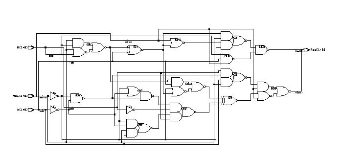
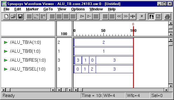
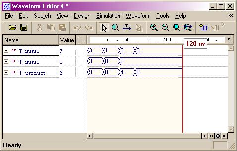
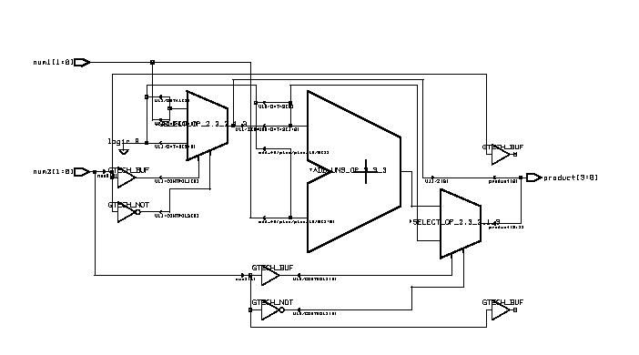
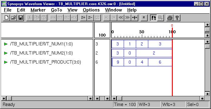
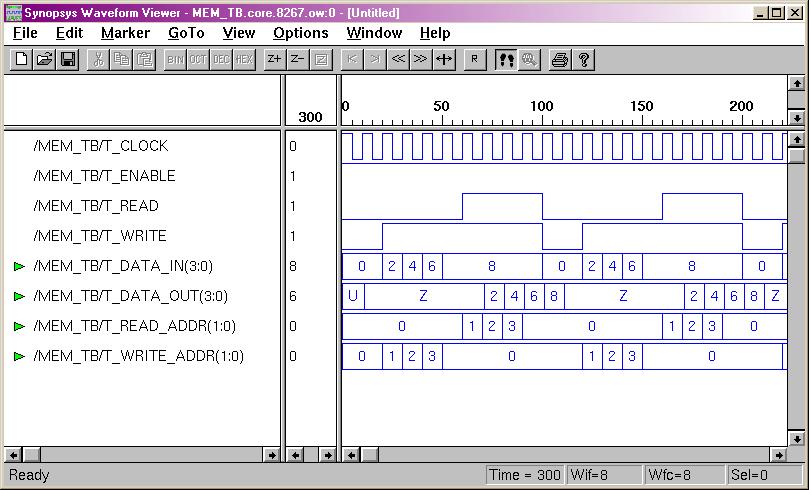
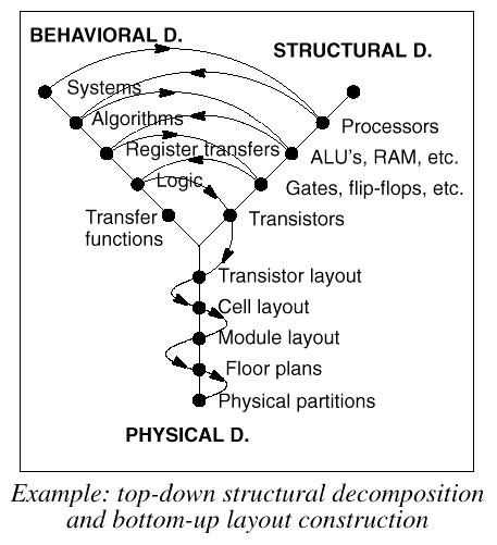
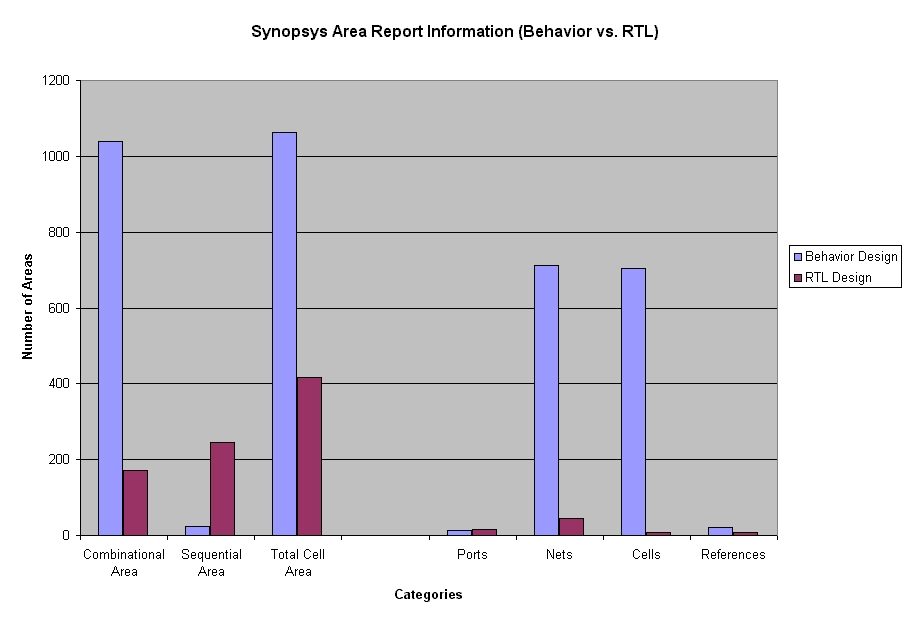
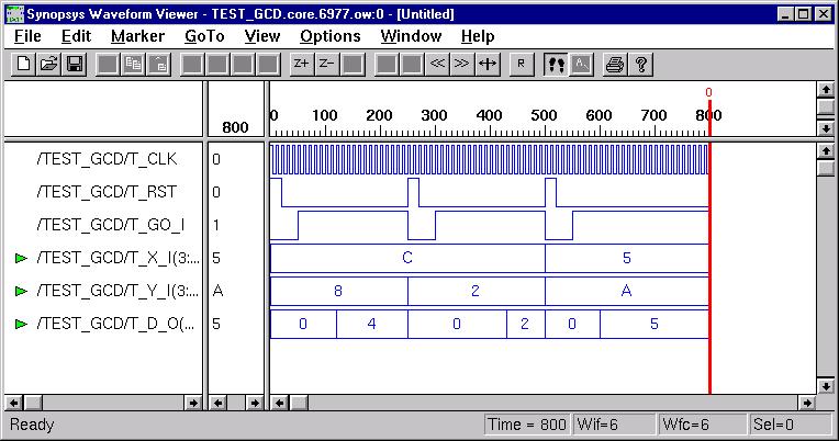
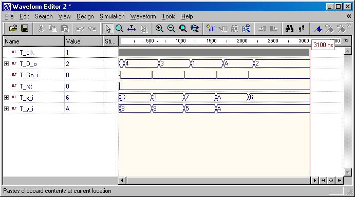
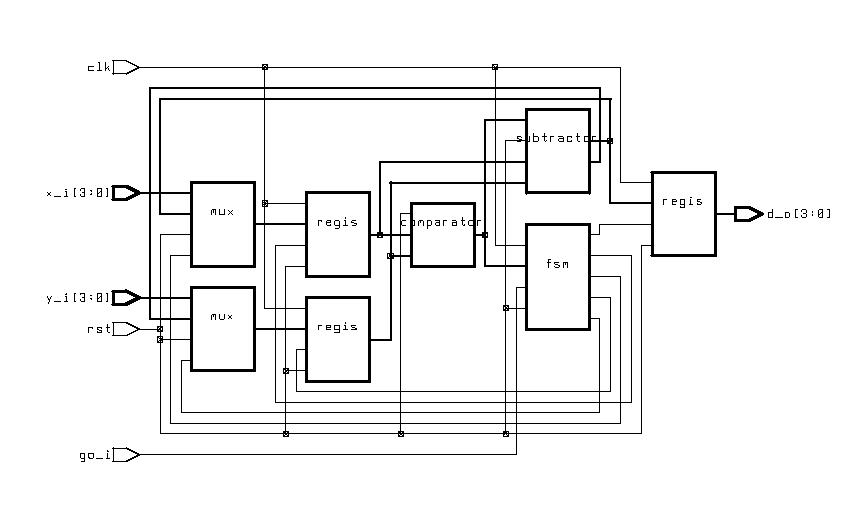
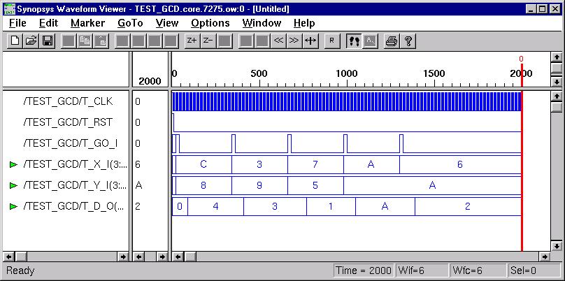
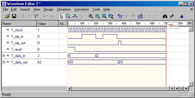
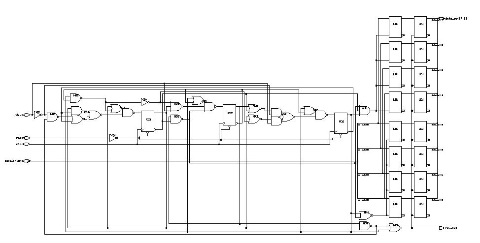
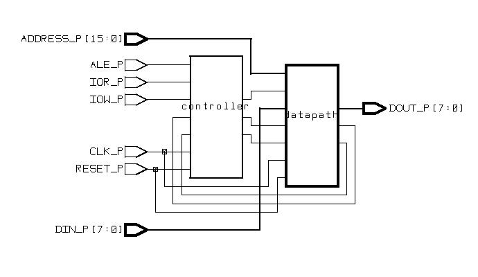
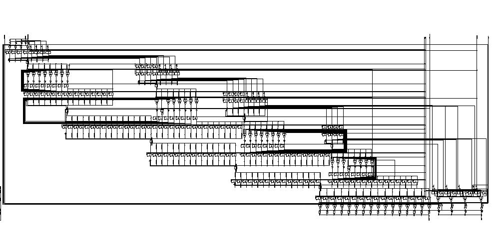
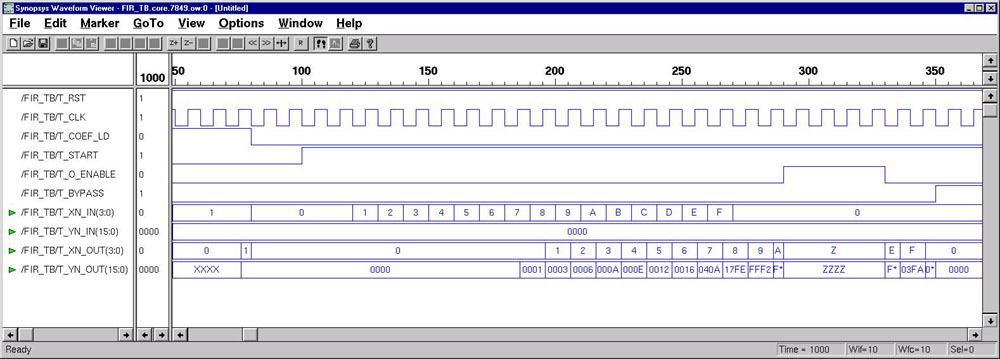
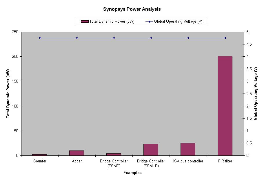
Custom Single-Purpose Processor Design (ESD Chapter 2, Chapter 4) The first three examples illustrate the difference between RTL FSMD model (Finite State Machine with Datapath buildin) and RTL FSM + DataPath model. From view of RT level design, each digital design consists of a Control Unit (FSM) and a Datapath. The datapath consists of storage units such as registers and memories, and combinational units such as ALUs, adders, multipliers, shifters, and comparators. The datapath takes the operands from storage units, performs the computation in the combinatorial units, and returns the results to the storage units during each state. This process typically takes one or two clock cycles. Data-flow (looks more like an Algorithm) modeling is presented in the fourth example. The FIR digital filter algorithm is simulated and synthesized using VHDL. A comparison of the coding styles between the RTL modeling and Algorithm level modeling highlights the different techniques.
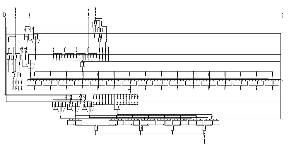
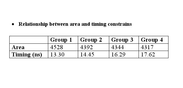
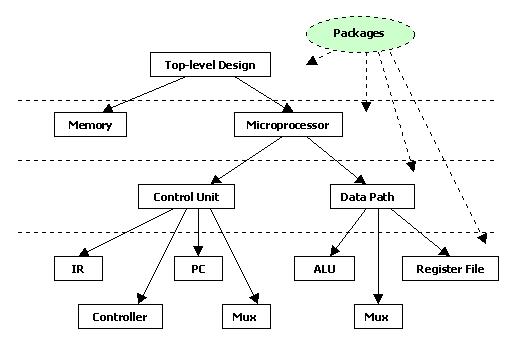
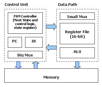
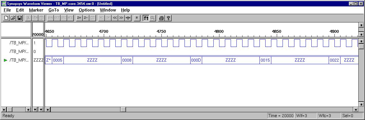
General-Purpose Processor Design (ESD Book Chapter 3, Figure 3.15) As indicated in the previous part, an Application Specific Integrated Circuit (ASIC) is specified with behavior descriptions which are presented in the form of particular algorithm or flowchart. A general purpose processor, on the other hand, is specified completely by its instruction set (IS). A sequence of instructions is required for the computation of a mathematical expression or any other similar computational task. To illustrate the whole procedure, a simple Pseudo-Microprocessor model is used which contains seven instructions (ESD book figure 3.7). The RT level design method from previous examples is used again to construct this microprocessor. The CPU will fetch, decode, and execute each instruction in order to get the final result. For test purposes, a short program (sequential instructions) is loaded into the memory. After execution, this program will obtain 10 Fabonacci Numbers, and store the results into specific memory address. The design was implemented using Active-HDL and Synopsys Design Compiler. (Please note that PC.vhd need a little modify to get correct synthesis result. Just a practice for the reader.)
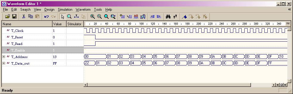
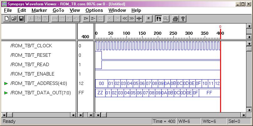
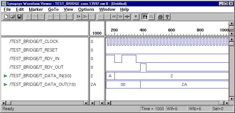
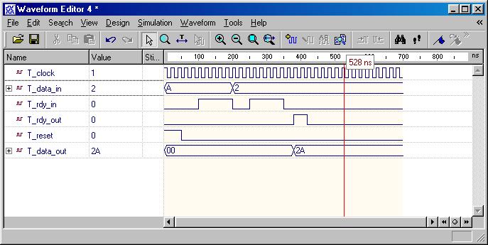
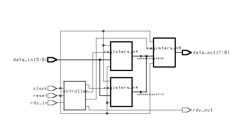
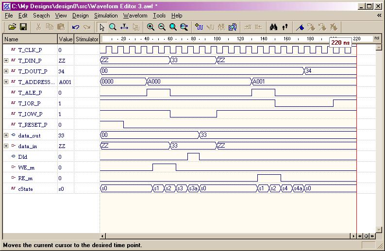
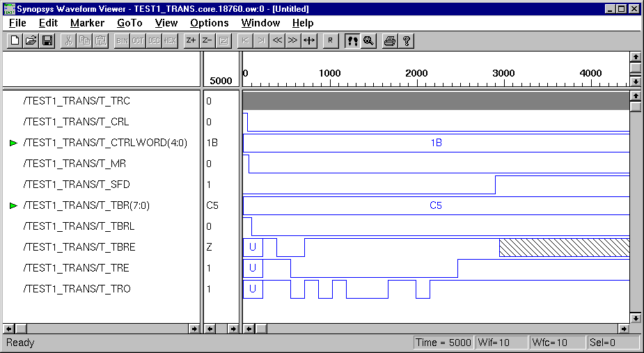
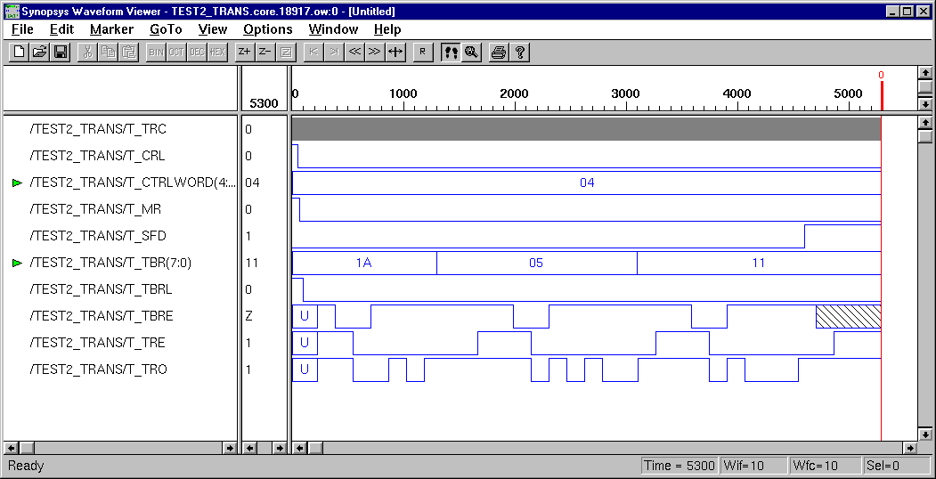
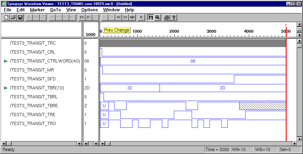
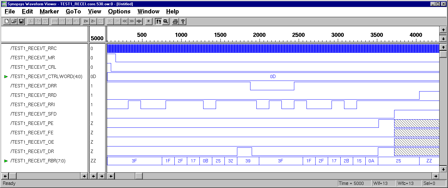
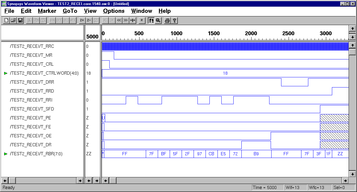
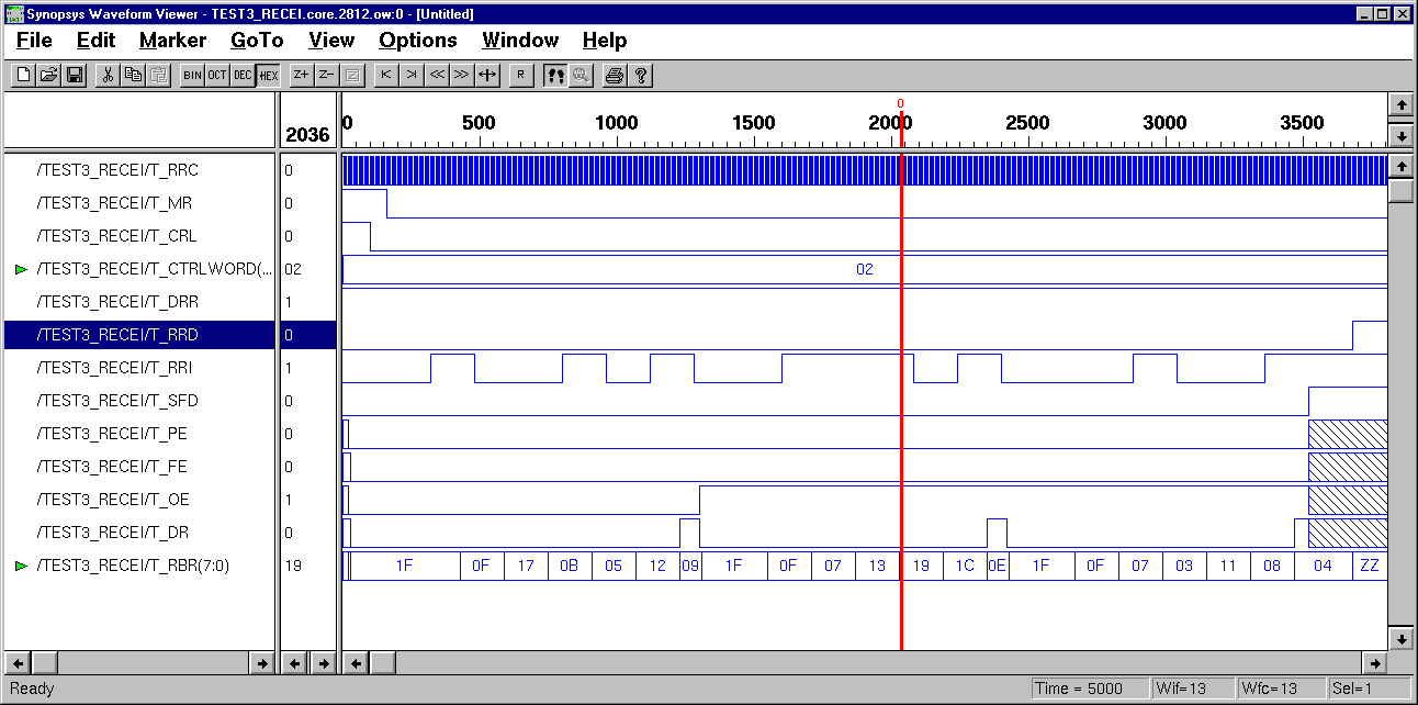
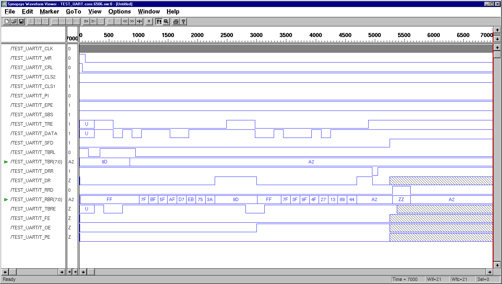
Appendix: Modeling a real industry chip - HD 6402 (ESD Chapter 4)
Created by Weijun Zhang (weijun_92507@yahoo.com) |

No comments:
Post a Comment